 Fraunhofer Center for Silicon Photovoltaics CSP
PV Recycling
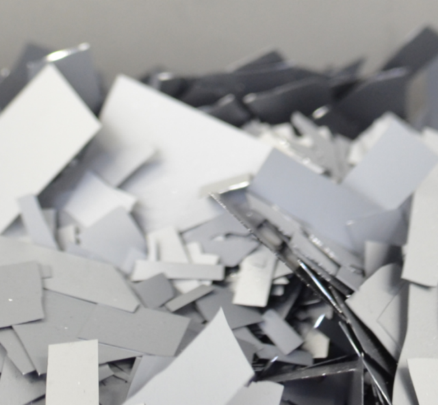

In order to be able to reuse the silicon of old pv modules, researchers from the Fraunhofer Center for Silicon Photovoltaics CSP together with the largest German recycling company for PV modules, Reiling GmbH & Co. KG, have developed a solution, in which the silicon in the discarded modules was recycled on an industrial scale and reused to produce new PERC solar cells.
more info© Fraunhofer CSP

The float-zone (FZ) method allows the growth of silicon crystals with excellent properties, especially with regard to oxygen concentration. In contrast to other growth methods, the oxygen concentration is more than two orders of magnitude lower here. This makes FZ crystals particularly interesting for use in power electronics.
more info© Fraunhofer CSP
Resource recovery from PV modules at the end of their life-cycle will move more and more into focus for the responsible consumption of raw materials and the energy efficient use of renewable feedstock. The Fraunhofer CSP develops new procedures for the refinement and the reuse of wafer and cell scrap, with the final goal to feed the PV silicon back into the value chain. High temperature melting furnaces are available, inductive heating allows fast heating-up and cooling down cycles. Wet chemical processes are under development to etch off surface coatings and to dissolve metallic impurities. New methods are investigated for segregation based refinement steps.
Furthermore, the use of getter processes or the application of inductive vacuum melting, or the treatment of liquid silicon with gas bubbling and with active stirring are techniques offered to remove impurities. Modern equipment for trace analysis gives a direct feedback with respect to the efficiency of the refinement process and a quantification of the material purification. The refined silicon might then be crystallized in our state-of-the-art industrial size crystallization equipment, like the Czochralski-pullers or the directional solidification furnace.

APOLLO project is funded by the European Union’s Horizon Europe research and innovation programme.
APOLLO is an acronym for "A Proactive Approach to the Recovery and Recycling of Photovoltaic Modules,".
The focus is on revolutionizing recycling practices for Photovoltaic (PV) waste modules.

End of Life Cycle of PV Modules: Processing of old modules and recycling of valuable substances into the material cycle
As part of the project, one ton of silicon is to be processed, 20 kg of silver recovered and glass returned to the glass basin.
In addition to the clean separation of the valuable materials and the processing of the metal-containing dusts, the focus will be on the recycling of the metals and silicon as secondary raw materials for PV production instead of re-using them only thermally.
Fraunhofer Center for Silicon Photovoltaics CSP, division »Crystallization Technologies«, provides a technology platform for industry related crystallization using production scale, state-of-the-art equipment. Our research activities focus on the reduction of process costs, the optimization of ingot properties, and further improvements of automation of crystallization processes.
Due to the competences of Fraunhofer CSP and the embedding into the Fraunhofer Institute for Solar Energy Systems ISE, the whole spectrum of silicon technology, from analytical methods, of material processing tools, wafering, cell manufacturing, through to cell certifications, and module fabrication is available.
Czochralski
With an EKZ-2700 and two EKZ-3500 (all from PVA-Tepla), Fraunhofer CSP has efficient and highly sophisticated Czochralski pullers for the growth of mono-ingots up to 9” diameter. The machines are equipped with optimized hot-zones, graphite cones and gate valves, which allow the growth of several ingots out of one crucible. The process is automated to a high degree, different recipes are available, e.g. for variations of the diameter, the shoulder angle, or the cone length. A feeder system for maximizing the charge weight or for tests related to multi-pulling may be used as well as a unit for active crystal cooling, which enhances the removal of latent heat during solidification allowing higher crystallization rates.
Research activities include questions related to the crucible life-time, the transport of oxygen into the crystal, and to the optimization of the process with respect to processing time and energy consumption. Further on, we are performing test crystallization experiments for leading silicon feedstock manufacturers in order to analyze the material quality and the resulting resistivity distribution up to the resulting cell efficiencies.
Float-Zone
With the FZ-14, we are able to grow Floating Zone crystals with a diameter up to 4“ and a length of 130 cm, with the newly developed FZ-35 processes up to 8” are possible. Our Floating Zone (FZ) activities focus on benchmark tests of different feedstock materials and the preparation of feed-rods from cheap solar-grade silicon regarding the use for float zone growth. A further topic is the improvement of the process automation and user friendliness. The advantages of the FZ technique are impressive, like higher growth rates, reduced oxygen and carbon concentrations, and cost savings on crucibles.
FZ-crystals usually show the highest carrier lifetimes (> 2-3 ms) and highest cell efficiencies of all silicon wafers. Nevertheless, for mainstream application of the FZ method, the process needs a much higher degree of automation than it is given right now. If a sufficient supply of feedstock usable for FZ is guaranteed, the FZ technique might become a serious competitor for the production of solar grade ingots. The FZ technique allows the rather simple in-situ doping from the gas phase. In such a way, very uniform axial dopant distribution profiles can be achieved, which is an important aspect with respect to the growth of phosphorous doped n-type material.

Vertical Gradient Freeze
Our multi-crystallizer VGF-732 is equipped with a G4 hot-zone, which allows the casting of 250 kg blocks. The machine is equipped with three independently controllable heaters, which allows a very flexible temperature control. The thermal flexibility is very favorable for the implementation of mono-like processes as well as the casting of high-performance silicon. The multi-crystallizer is primarily used for the realization of specific R&D programs for process optimization, like e.g. improvement of the temperature control, reduction of carbon impurity level by adapted gas flow direction and gas flow rates. Another current topic is the development of new methods for the detection of the solid-liquid interface and the in-situ measurement of the crystallization rate. For smaller ingots, a G1/G2 furnace is available at the Fraunhofer ISE in Freiburg. A dedicated crucible coating facility is fully operational. With this machine, ingots of some 20 to 80 kg can be grown.
The vacuum induction melting facility is used in particular for R&D topics related to material refinement and recycling of cell and module scrap. New processes for silicon purification and the re-use of recycled silicon for the ingot and wafer manufacturing are under development.
")