Optics and Laser

µ-TLM structure
© Fraunhofer CSP
Detailed view of two troughs of a µ-TLM structure in LSM height profile imaging.

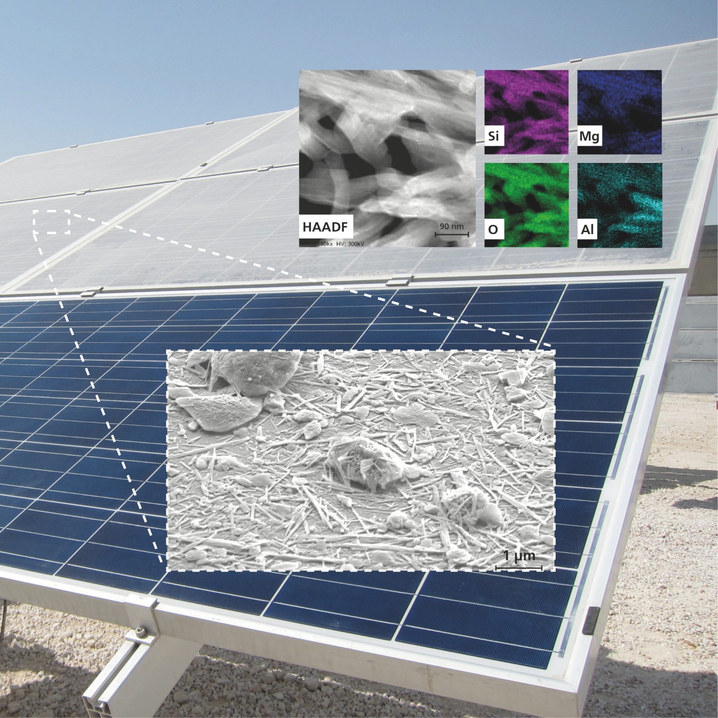
Failure diagnostics and nanoscopic examinations of thin-film solar modules require extremely high-resolution analytics. Electrical, optical and microstructural methods are continuously further developed in order to evaluate processes and materials in thin-film photovoltaics (CdTe, CIGS, Si, OPV). We determine the reliability of thin-film solar modules based on spatially resolved yield/loss analyses and analyze the cause of failures in open-field and laboratory installations. We design and manufacture special test structures by applying laser structuring and coating technology.

Partners from the PV industry, plant operators, and equipment manufacturers are the ones who define the R&D objectives. By applying electro-optical localization and preparation methods and material-scientific analytics, the causes for defects can be elucidated down to their atomic dimensions in a very short time. Based on a fundamental understanding of the processing conditions and the resulting electrical properties of the material the team Thin Film Characterization develops proposals for »inline« diagnostics.

Services

  • Defect diagnostics in thin-film PV: localization, target preparation and microstructural analysis
  • Element analytics in film stacks: quantitative depth-profile analyses with TOFSIMS, XPS, TEM
  • Laser structuring and contract coating (TCOs, rear contacts)
  • Electrical micro characterization
  • Optical simulation/characterization

Examples

Electro-optical methods and REM/EBIC
© Fraunhofer CSP
Electro-optical methods and REM/EBIC (a) help to localize defects and contaminations in thin-film solar cells. Target preparation methods permits the identification of defects buried in the layer structure (b) and to draw conclusions on process faults.

Defect Diagnostics in Crystalline Si Thin Films

Defects and contaminations in in thin-film solar cells are localized by applying electro-optical methods and REM/EBIC (a). Target preparation methods permits the identification of defects buried in the layer structure (b) and to draw conclusions on faults in processing. More advanced element-analytical methods like ToF-SIMS, XPS, TEM/EDX help to classify the various defect types.

characterization of dust-soiled glass in a test field in Qatar
© Fraunhofer CSP
REM, FIB, TEM & EDX characterization of dust-soiled glass in a test field in Qatar.

Anti-Soiling Evaluation of Glass Coating

In regions with high airborne dust loads (e.g. deserts, cities) dust depositions on the glass surfaces of PV modules are the cause significant yield losses. Anti-soiling layers, for example, can be applied to minimize the otherwise necessary cleaning effort. A characterization of the microstructure is useful for understanding and testing the function of these dust-repellent layers. For example, under real desert conditions, cementation processes occur in which dust particles are virtually "caked" onto the glass surface. We realize the simulation of such soiling processes in the laboratory with the aid of a test facility which has been developed exclusively for this purpose.

CIGS layer
© Fraunhofer CSP
Atomically resolved structure of the CIGS layer.

Stacking Faults in the Atomic Structure of CIGS Films

We produce artifact-free cross-sections of susceptible thin-film systems such as CIGS solar cells and apply preparation methods especially developed for this purpose. They allow for the high-resolution imaging of the atomic structure by transmission electron microscopy (TEM). The images reveal local material defects as irregularities in the ordered crystal structure of the atoms.