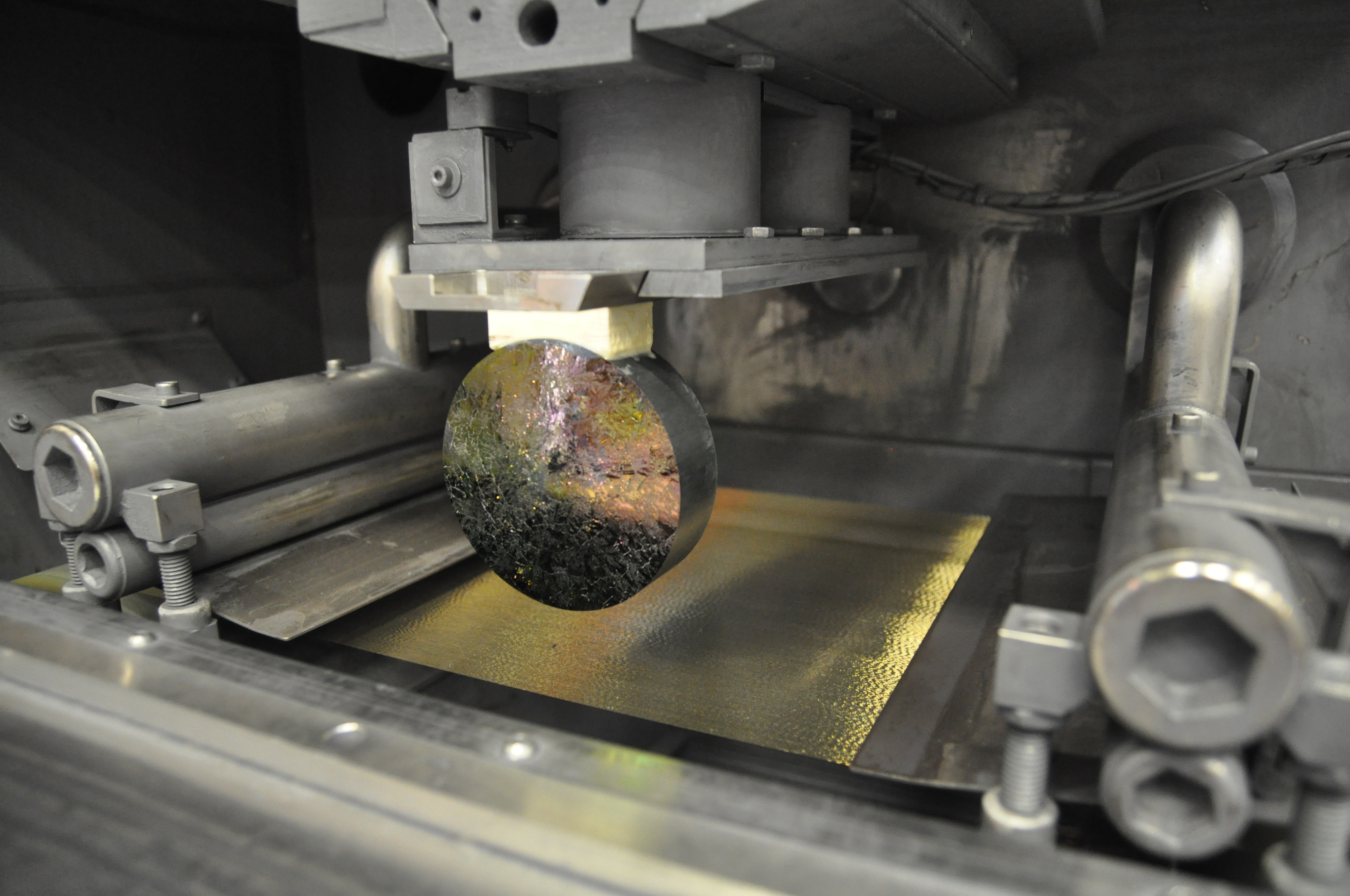
Multi-wire sawing technology enabling the sawing of extremely hard materials such as silicon carbide
The multi-wire sawing process originated in the semiconductor industry. Microelectronic wafers are manufactured from monocrystalline silicon ingots using wire saws. This technology has been successfully transferred to other industries and materials. Today, in addition to silicon, sapphire, silicon carbide, quartz glass and other brittle-hard materials are also cut into wafers using multi-wire saw technology. The microstructure and / or the hardness of the different materials represent the greatest challenge. Thanks to the process know-how and technical capabilities available at the Fraunhofer CSP (real-time monitoring of the sawing process, rocking unit for minimizing the contact surface during sawing), it was also possible to cut extremely hard materials such as silicon carbide into wafers. The illustrations show a silicon carbide crystal (diameter 100 mm) which was sawn into wafers of high surface quality.
 Fraunhofer Center for Silicon Photovoltaics CSP