Diagnostics and Metrology Solar Cells

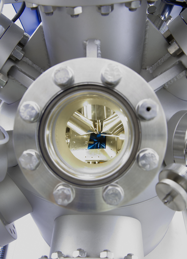
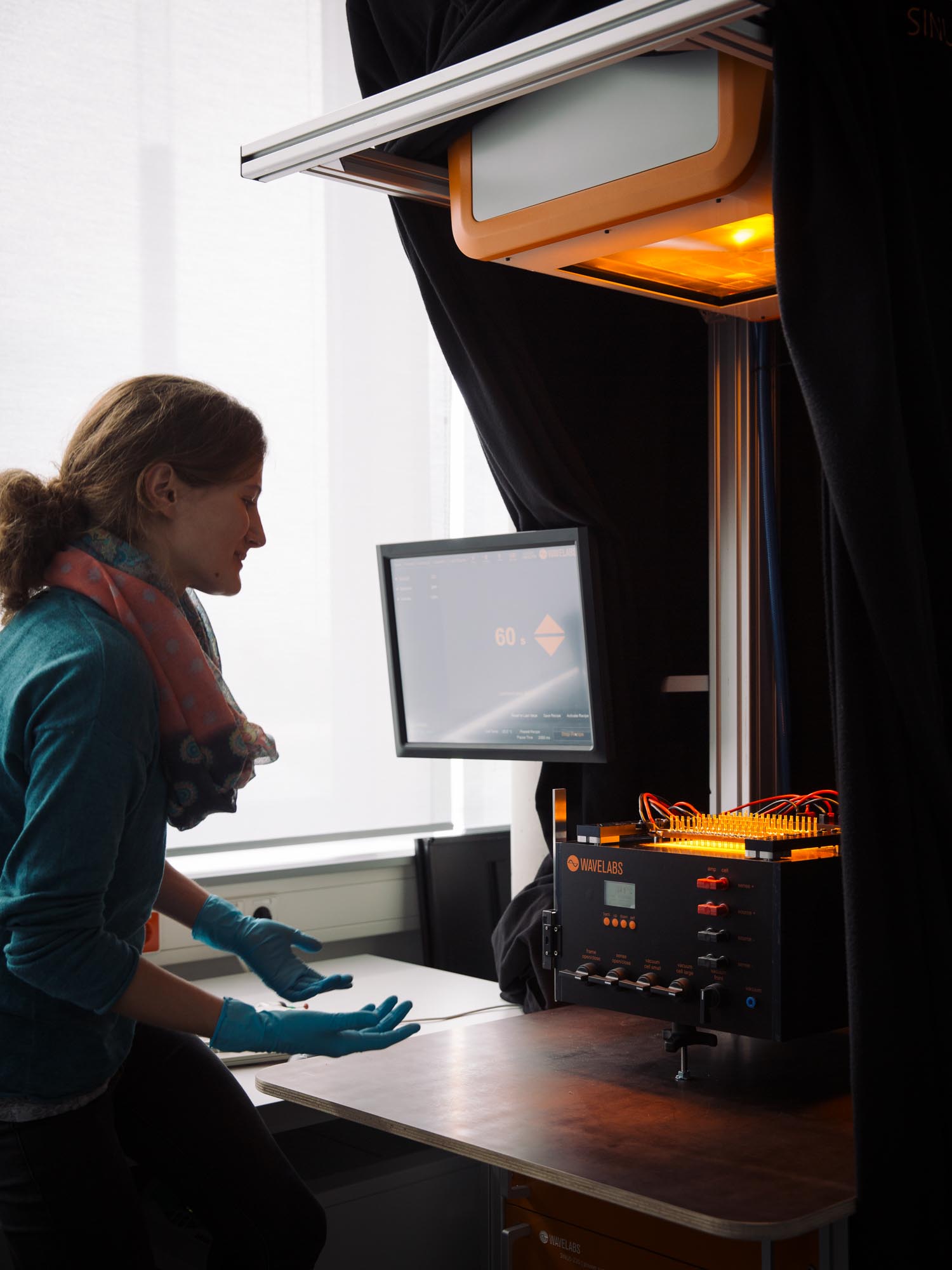
Performance, reliability and cost efficiency are the decisive characteristics of a perfect solar cell. The »Diagnostics of Solar Cell« group is working on these issues, supported by industrial sponsors and partners in research and development. The teams »Electric Characterization«, »c-Si Defect Diagnostics« and »Thin-film Characterization« set the standards for quality assurance and failure analysis in photovoltaics. To this end, a broad spectrum of material-scientific methods are available – ranging from trace element analytics over quantum efficiency all the way to atomic microstructure diagnostics.

Research activities span from the characterization of the crystalline solar silicon to the microstructure-based failure diagnostics for the thin-film photovoltaic industry. In addition, new layer systems and laser structuring methods are being developed for the next generation of solar cells.


We offer:

  • Rapid testing tools for module defects such as PID
  • Electric characterization of solar cell, wafers and blocks
  • Microstructure diagnostics on crystalline solar cells


Thin Film-PV: Micro Analytics and Laser Processing

We determine the reliability of thin-film solar modules by means of spatially resolved yield/loss analyses and causal research into failures in open-field and laboratory installations. We design and manufacture special test structures using laser structuring and coating technology.


Electrical Characterization

Hohe Effizienz und lange Lebensdauer sind zwei der zentralen Anforderungen an innovative Photovoltaikprodukte. Für die quantitative Bewertung kommen am Fraunhofer CSP innovative Labormessverfahren für Solarzellen und -module in Kombination mit statistischer Datenauswertung, Modellierung und numerischer Simulation zum Einsatz.


Silicon Filters and Analytics for Micro- and Nanoplastics

In addition to providing individually adapted filter materials and corresponding accessories for conducting filtration experiments, we offer our customers various analytical tests on filter substrates in order to evaluate water samples and the particles they contain, in addition to laboratory tests at Fraunhofer CSP.

Equipment Development

 testing equipment PIDcon
© Fraunhofer CSP
Thanks to the testing equipment PIDcon potential-induced degradation (PID) can be detected already on solar cell level.

c-Si Defect Diagnostics

Thin Film Characterization
© Fraunhofer CSP
  • Metallography, ion and laser beam assisted sample preparation tools
  • ns laser structuring (1064 nm, 566 nm, 355 nm)
  • inkjet printing
  • Microscopy (optical, NIR, module microscopy)
  • Electroluminescence Microscopy (EL, µEL)
  • Lock-in Thermography
  • Laser Scanning Microscopy
  • Analytical scanning electron microscopy (SEM) with EDX, EBSD, EBIC
  • Transmission electron microscopy (TEM) with EDX
  • Focused ion beam (FIB)
  • Time of flight secondary ion mass spectrometry (ToF-SIMS)
  • X-ray photo electron spectroscopy (XPS)
  • Scanning probe microscopy (AFM/SPM)
  • Electrical micro probe characterization
  • Scanning acoustic microscopy (SAM)

Thin Film Characterization

UHV chamber of the ToF-SIMS
© Fraunhofer CSP
In the UHV chamber of the ToF-SIMS the chemical composition of a sample is determined with the aid of ion-sputtering sources.
  • Metallography, ion and laser beam assisted sample preparation tools
  • ns laser structuring (1064 nm, 566 nm, 355 nm)
  • Inkjet printing
  • Microscopy (optical, NIR, module microscopy)
  • Electroluminescence Microscopy (EL, µEL)
  • Lock-in Thermography
  • Laser Scanning Microscopy
  • Analytical scanning electron microscopy (SEM) with EDX, EBSD, EBIC
  • Transmission electron microscopy (TEM) with EDX
  • Focused ion beam (FIB)
  • Time of flight secondary ion mass spectrometry (ToF-SIMS)
  • X-ray photo electron spectroscopy (XPS)
  • Scanning probe microscopy (AFM/SPM)
  • Electrical micro probe characterization
  • Scanning acoustic microscopy (SAM)

Electrical Characterization

sun simulator WaveLabs Sinus-220
© Fraunhofer CSP
With the sun simulator WaveLabs Sinus-220, we are able to measure the current efficiency at different light wavelengths.
  • Injection-dependent carrier lifetime (Si-block, -wafer)
  • Carrier-lifetime mapping (Si-block, -wafer)
  • Conductivity measurements (four-point, eddy current)
  • Position resolved electroluminescence (cells and mini-modules)
  • Position resolved photoluminescence (si-blocks, -wafers, solar-cells, mini-modules)
  • Position-resolved lock-in-thermographie (solar-cells, mini-modules)
  • Light-induced local currents LBIC (solar-cells, mini-modules)
  • Internal and external quantum efficiency (solar-cells, mini-modules)
  • Chracterization of passivation layers
  • Doping profiles based on resistivity
  • Current-voltage-curves and parameter extraction (solar-cells, mini-modules)
  • Solar simulator